Semiconductor Automation Solutions for Precision Manufacturing
How Advanced Industrial Automation Revolutionizes Semiconductor Manufacturing
The Semiconductor Industry’s Growing Automation Demands
Global semiconductor manufacturing requires unprecedented precision. According to Statista, the market will reach $1.38 trillion by 2029. This growth drives demand for sophisticated automation solutions. Festo’s integrated approach addresses these complex manufacturing challenges effectively.
Revolutionary Wafer Handling with Smart Gantry Systems
Festo’s central hub features an innovative inverted gantry system. This solution replaces traditional SCARA robots in many applications. The system handles wafers from FOUP carriers with exceptional precision. Key advantages include:
- Cost-effective alternative to conventional robot systems
- High-speed wafer transfer capabilities
- Integrated alignment functionality
- Sub-micron positioning accuracy
The integrated wafer aligner combines gripping and alignment functions. This innovation significantly reduces system complexity.
Precision Coating and Chemical Processing Solutions
Module 1 demonstrates advanced wet chemical processing. The system begins with comprehensive FOUP purging. Festo Mass Flow Controllers ensure contaminant-free environments. The coating station utilizes innovative technology:
- Electric linear axes provide precise nozzle movement
- “Suck-back” solutions prevent chemical dripping
- Even coating distribution reduces material waste
- Consistent process quality enhances yield rates
These industrial automation features maintain process integrity throughout.
Vacuum Processing and Micro-Positioning Excellence
Module 2 showcases vacuum environment capabilities. This includes critical dry etching processes. The system demonstrates sophisticated valve control:
- Gentle slit and gate valve operation
- Smooth wafer transitions into vacuum chambers
- Pneumatic pin lift systems for precise placement
- Micrometer-level positioning accuracy
These features ensure reliable performance in sensitive processes.
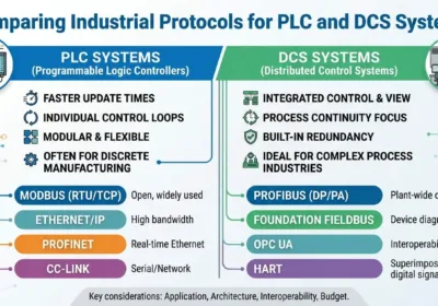
Integrated Control Systems for Semiconductor Manufacturing
Modern semiconductor facilities require seamless integration. Festo’s approach combines multiple automation technologies:
- PLC systems coordinate overall equipment control
- DCS solutions manage process parameters
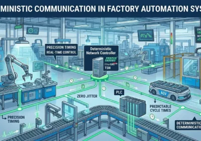
- Factory automation networks enable real-time monitoring
- Digital twins facilitate process optimization
This integrated control architecture maximizes equipment effectiveness.
Expert Analysis: The Future of Semiconductor Automation
From PLCDCSHUB’s perspective, this demonstration highlights crucial trends. Semiconductor manufacturers increasingly adopt integrated automation solutions. The industry shift toward smarter factory automation continues accelerating. Key observations include:
- Combined functionality reduces system footprint
- Integrated control systems enhance reliability
- Precision handling solutions improve yield rates
- Modular designs support future expansion needs
These developments align with Industry 4.0 implementation strategies.
Practical Implementation Guidelines
Manufacturers considering similar automation upgrades should:
- Conduct thorough process requirement analysis
- Evaluate integration capabilities with existing systems
- Consider long-term maintenance and support needs
- Plan for future scalability and technology upgrades
Proper planning ensures successful automation implementation.
Connecting Innovation to Practical Applications
Implementing advanced semiconductor automation requires expert guidance. For manufacturers seeking integrated control solutions, PLCDCSHUB provides comprehensive industrial automation expertise. Our experience helps optimize semiconductor manufacturing processes effectively.
Frequently Asked Questions
- What advantages do inverted gantries offer over SCARA robots? They provide comparable precision with lower cost and integrated alignment capabilities.
- How do mass flow controllers improve semiconductor manufacturing? They ensure precise gas control for contamination-free processing environments.
- Why is micrometer-level positioning critical in semiconductor applications? It ensures proper alignment and placement for nanoscale manufacturing processes.
Related Posts