SWIR Cameras for Semiconductor Inspection & Automation
SVS-Vistek SWIR Cameras Revolutionize Semiconductor Quality Control
Semiconductor manufacturers face increasing quality challenges. Subsurface defects can compromise chip performance. Traditional inspection methods often miss hidden flaws. SWIR technology provides the solution.
The Semiconductor Inspection Challenge
Modern chips require flawless silicon wafers. Subsurface defects remain invisible to standard cameras. These hidden flaws can cause catastrophic failures. Therefore, advanced inspection becomes essential.
The global semiconductor market reaches $728 billion annually. According to World Semiconductor Trade Statistics, demand continues growing. AI and computing applications drive quality requirements higher.
SWIR Technology Advantages
Short Wavelength Infra-Red cameras penetrate silicon surfaces. They visualize internal structures clearly. Wavelengths around 1,100 nm reveal hidden defects. These include micro-cracks and impurities.
- Detects subsurface defects invisible to visible light
- Penetrates silicon with 1,100 nm wavelengths
- Reveals micro-cracks and particle contamination
- Works with standard C-Mount lens systems
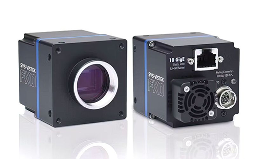
SVS-Vistek Camera Specifications
SVS-Vistek SenSWIR FXO cameras offer advanced features. They provide resolutions to 5.2 megapixels. The extended wavelength range covers 400-1700 nm. This enables simultaneous SWIR and visible imaging.
Camera models include specific capabilities:
- SenSWIR FXO 992: 5.2MP at 132 frames per second
- SenSWIR FXO 993: 3.1MP at 173 frames per second
- 3.45 µm pixels capture minute details
- Two-Point Non-Uniformity Correction enhances accuracy
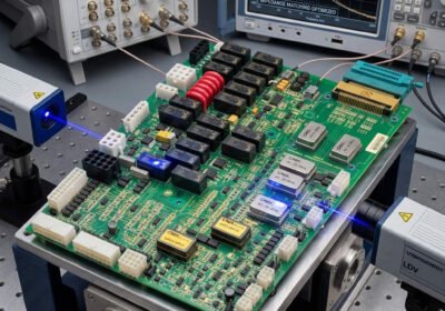
Industrial Automation Integration
These cameras integrate seamlessly with factory automation systems. 10GigE Vision and CoaXPress interfaces ensure compatibility. They connect directly with PLC and DCS control systems. This enables automated defect detection workflows.
According to PLCDCSHUB analysis, “Machine vision integration with control systems becomes crucial for smart factories. SWIR technology represents the next evolution in industrial automation.”
Technical Performance Features
SVS-Vistek cameras include sophisticated thermal management. This ensures consistent image quality. Thermoelectric Cooling reduces sensor noise. The Peltier effect actively controls temperature.
Additional technical advantages include:
- Integrated 4-channel strobe controller
- GenICam 3.0 and GenTL standardization
- Outstanding dynamic range and homogeneity
- Reduced dark current through active cooling
Market Applications and Trends
Semiconductor inspection demands continue increasing. MarketsandMarkets predicts strong machine vision growth. The technology serves multiple industrial sectors. Factory automation benefits significantly.
Key application areas include:
- Semiconductor wafer inspection
- Solar cell manufacturing quality control
- Pharmaceutical packaging verification
- Food sorting and contamination detection
Implementation Scenarios
Manufacturers can deploy SWIR technology effectively:
- Automated Wafer Inspection: Integrated with PLC systems for continuous monitoring
- Quality Control Stations: Connected to DCS for real-time process adjustment
- Research Laboratories: High-resolution analysis for development teams
- Production Lines: Factory automation with instant defect detection
For advanced industrial automation solutions incorporating machine vision technology, explore PLCDCSHUB’s comprehensive product range featuring integrated control systems and quality monitoring solutions.
Industry Impact and Future Outlook
SWIR technology transforms semiconductor manufacturing. It enables previously impossible inspections. Quality improvements directly impact yield rates. Production efficiency increases significantly.
The technology continues evolving. Higher resolutions and faster processing emerge regularly. Integration with industrial automation systems deepens. Smart factories benefit most from these advances.
Frequently Asked Questions
How does SWIR technology improve semiconductor yield?
SWIR cameras detect subsurface defects before processing. This prevents wasted resources on flawed wafers. Early detection significantly improves overall yield rates.
Can existing factories integrate SWIR inspection systems?
Yes, most systems connect through standard industrial interfaces. They integrate with common PLC and automation platforms. Retrofitting typically requires minimal modifications.
What industries beyond semiconductors use SWIR technology?
Multiple sectors benefit from SWIR capabilities. These include solar manufacturing, food processing, pharmaceuticals, and electronics assembly. Any application requiring subsurface inspection can utilize this technology.
Related Posts